Technology
SIMPLE SCIENCE
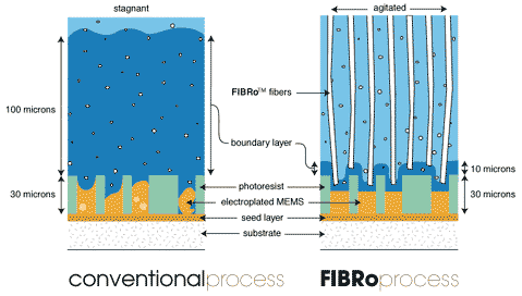
This is electrochemistry, not rocket science: get the metal from the solution to the cathode with a uniform thickness. Theoretically, plating can be done right in one try, not ten. But, you have thousands of nasty variables to contend with. What we’ve done is eliminate many of those variables, and found ways to control others. We focused mainly on where the actual plating occurs: the interface’s boundary layer. And, with a little innovation, we mastered it.
How?
ECSI Fibrotools’ proprietary FIBRotools (Fiber-Initiated Boundary-layer Removal) process utilizes a unique fibrilic applicator to agitate and effectively reduce the boundary layer by up to 90%. The process control extends to the interface. You achieve uniformity, like clockwork. Simple. Practical. Repeatable.
UNMATCHED VERSATILITY
Nowadays micro and nano features are the main building blocks responsible for the explosion of modern technology. The limitless variety of the features and ambitious R&D efforts often require a multidisciplinary approach to micro and nano structure design and fabrication. With an exceptional flexibility and adaptability to process modification, FIBRotools™ can be employed in a wide variety of thin and thick film electroplating conditions and parameters.
As a result, FIBRotools™ enable numerous processes for uniform, reproducible, precision micro and nano structure design, fabrication and testing over 2” to 8” substrates. Based on its proven FIBRotools™ technology, ElectroChemical Systems, Inc. (ECSI Fibrotools) is now offering:
Fast track scale-up development from chips and 2” substrates to 8” substrates of various shapes and thickness
Electroplating under magnetic field
Silicone seedless electroplating
Electroplating with laser
Electroplating under ultrasound
Electroplating with a combination of selected spot laser exposure
Electroplating in a combination of magnetic field and laser
Combination of seedless electroplating under magnetic field
Micro/macro uniformity less than 5% across the wafer
Electrophoresis of organic and inorganic matter
APPLICATION
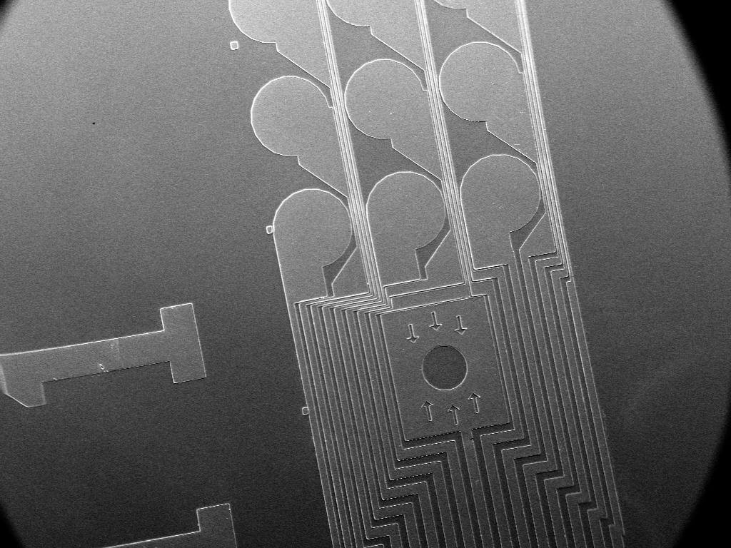
Retinal Implant
The versatility of FIBRotools™ technology makes IKo™ Electroplating Systems suitable for a wide range of thin and thick film applications.
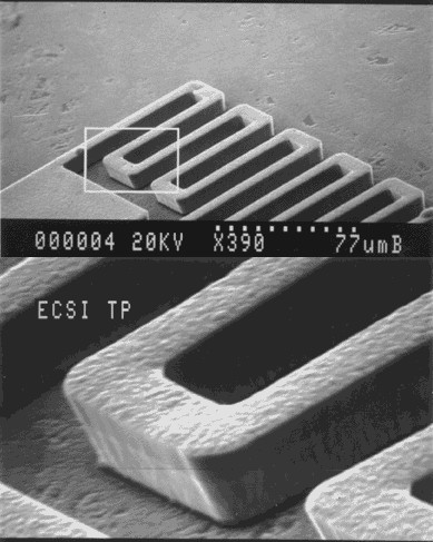
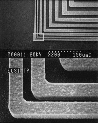
15µ electroformed Cu
interconnects on silicon
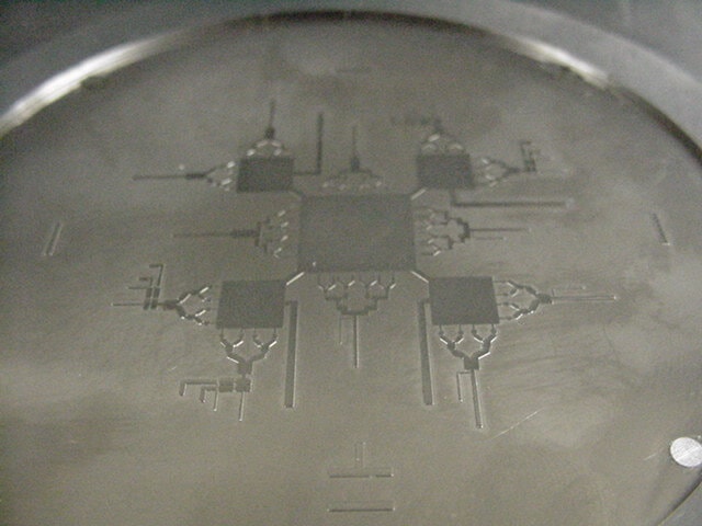
Electroformed BioMEMS mold
for embossing
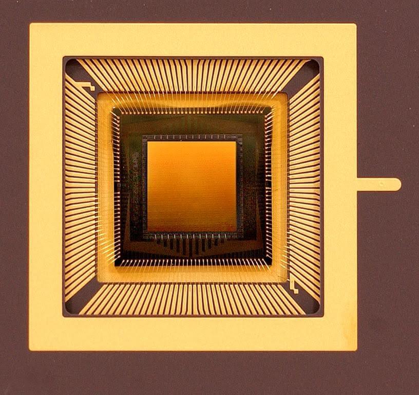
Deformable mirror
Uniform and Reproducible Electroplating
- Uniform electroplating of patterned or plain substrates in the nanometer to 100 plus micron range
- Fast track scale-up development from chips and 2” substrates to 8” substrates of various shapes and thickness
- MEMS, NEMS, and Nanostrutures
- Nanowire R&D
- Precision electroplating of alloys
Micro- and Nanoscale Silicone Modification
- Seedless electroplating
- Ferroelectric embodiment
- Optoelectronic effects
- Photonics effects
- Solar cells optimization
Electroforming Molds for Micro- and Nano-embossing
- Disposable Bio-chips / Bio-MEMs
- Micro- and nano-fluidics
- Microsensors
- Multi-phase flow R&D
Magnetic Alloy Deposition
- CoFe and CoNi Fe
- With or w/o magnetic field
Biomedical Research
- Bio-NANO interface development
- Nanowire combination with electrophoresis
- Retinal implants
Micro- and Nanorobotics
- Untethered mobile microrobots (video)
Flexible Electronics
- Deformable mirror (see picture above)