Discover CET
The Disruptive Technology for PWBs and flexible electronics.

WHAT IT DOES:
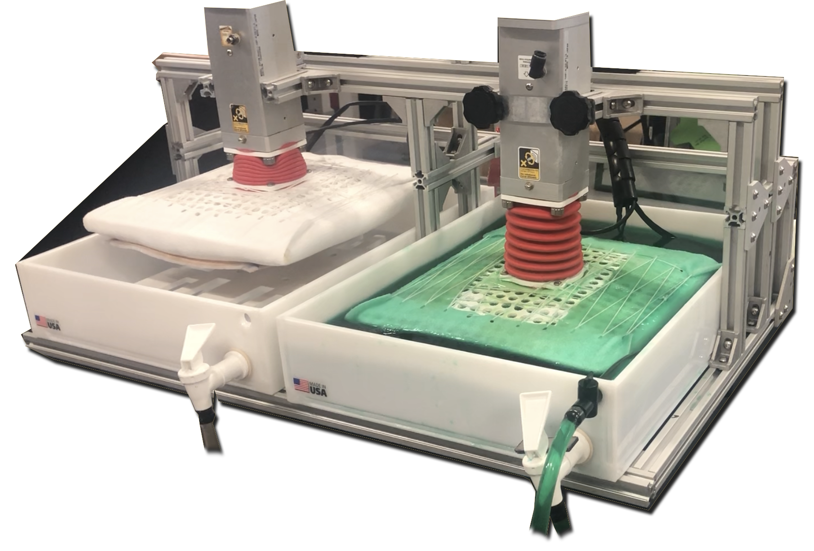
The Contact Electroplating Technology (CET) enables metallization of isolated electronic patterns by electroplating, without sacrificing the substrate real-estate for establishing direct contact to the power supply. The best way to form or deposit isolated microscopic and nano features in electronics is by electroplating if possible. The current state-of-the-art technology is not able to provide that. Contact Electroplating Technology (CET) (US Patent #10,184,189) patterns this efficiently, including PWBs and Flexible Electronics.
HOW IT DOES IT:
CET is a disruptive technology that interjects between the power supply and the electroplated micro and nano electronic structures. By using this proprietary process, we can contact isolated patterned electronic features with up to 5 million contacts per square inch. Those contacts allow electroplating of PWBs and Flexible Circuits within the electroplating solution. Following a high-speed xeroxing or patterning of isolated flexible structures with a layer of negligible thickness and resistance as high as several kiloohms cm, CET enables upgrading of the patterns by depositing desired thickness of pure metal, up to 10 microns. Completely isolated electronic interconnects with spacing as low as 25 microns. Completely isolated electronic interconnects with spacing as low as 25 microns are uniformly electroplated within seconds.
APPLICATIONS OF THE TECHNOLOGY:
CET is the latest technology to be developed by ECSI Fibrotools. Currently we have identified three major categories where CET will be wildly successful. Working with innovators like you, we can discover even more potential applications.
PWB
– PWB design can be simplified while reducing the volume of chemicals used and the environmental impact of processing
– Ni, Ag, Au, and other alloys can be electroplated without direct contact to the power supply, resulting in superior PWB performance and elimination of “black pads”
Wafer Plating
– Wafers can be patterned with isolated functional patterns without a seed layer
– Peripheral electrical contacts are eliminated
– Maximizes available space for patterning devices and interconnects
Flexible Electronics
– Deposition rate is identical to conventional electroplating, so a conveyorized system for flexible circuits can deliver high-throughput superior to ink-jet or paste
– Fully functional flexible circuits with feature densities of 25 microns or less can be fabricated
RESULTS:
Novel advanced design PWBs with better usage of the surface area free from the ubiquitous electrical contacts are now possible. Moreover, you can minimize the use of electroless or immersion processes thus minimizing the negative effect of environmentally harmful chemicals. With CET, you can cut the cord to the power supply and utilize less chemicals, which is great not only for your wallet, but for Mother Nature too.
