Meet IKo
Compact. Inexpensive.
And it works.

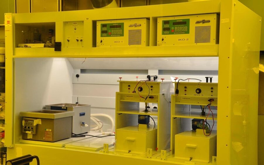
ECSI Fibrotools designs, builds, and supplies efficient, precision benchtop equipment for electroplating of MICRO- and NANO-structures. FIBRotools™ are an ideal solution for academic and R&D institutions seeking rapid optimization of novel designs for MEMS and NANO structures and advanced high-density interconnects (HDI). Publish and commercialize innovations faster with our uniform, reproducible electroplating process..
What enables us to do this at a low cost is our proprietary FIBRotools™ Fiber-Initiated Boundary-layer Removal technology. Complemented by our advanced wafer-holder design, FIBRotools™ produces uniformity, eliminates bubbles and minimizes edge effects.
FIBRotools™ is based on the work of our founder and CEO, Dr. Igor V. Kadija, whose discoveries in the physicochemical hydrodynamics of wet processing were awarded three US patents with worldwide patent coverage.
Flexible and adaptable to many different process configurations, FIBRotools™ enables fast track R&D in design advancements of a wide variety of MEMS, NANO, and HDI devices.
Discover CET
The disruptive technology for PWBs and flexible electronics
The Contact Electroplating Technology (CET) enables metallization of isolated electronic patterns by electroplating, without sacrificing the substrate real-estate for establishing direct contact to the power supply.
The best way to form or deposit isolated microscopic and nano features in electronics is by electroplating if possible. The current state-of-the-art technology is not able to provide that. Contact Electroplating Technology (CET) (US Patent #10,184,189) patterns this efficiently, including PWBs and Flexible Electronics.

